Chiplets Instead of Monolithic Processors: Why the Industry Is Moving to Modular Architecture
The semiconductor industry is undergoing one of its most significant architectural changes since the introduction of multi-core processors. For decades, manufacturers relied on large monolithic chips that integrated all major functions onto a single piece of silicon. As manufacturing processes became more complex and expensive, this approach started to encounter practical and economic limitations. By 2026, chiplet-based designs have become a central strategy for companies such as AMD, Intel, Apple, NVIDIA and several data-centre hardware suppliers. Instead of building one massive processor, engineers increasingly combine multiple specialised silicon blocks into a single package. This modular approach improves manufacturing efficiency, supports faster innovation and allows hardware designers to tailor products to specific workloads.
The Limitations of Traditional Monolithic Processors
A monolithic processor places computing cores, cache, memory controllers and other components on one large silicon die. While this method simplifies internal communication, it becomes increasingly difficult to manufacture as transistor density rises and process technologies shrink below 5 nm and 3 nm. Even a minor defect during production can render an entire chip unusable, reducing manufacturing yield and increasing costs.
The financial challenge has become particularly important. Modern fabrication facilities require investments measured in tens of billions of pounds or dollars. Producing larger dies on cutting-edge nodes significantly increases production expenses, making it harder for manufacturers to maintain profitability while delivering performance improvements.
Another issue involves design flexibility. Different processor components often have different requirements. CPU cores may benefit from the most advanced manufacturing process available, while input/output controllers, memory interfaces and networking logic can operate efficiently on more mature and less expensive nodes. A monolithic design forces all elements onto the same process technology, even when that is not the most efficient choice.
Why Scaling Challenges Accelerated the Search for Alternatives
For many years, Moore’s Law helped drive predictable performance gains. However, each new generation of manufacturing technology now delivers smaller improvements while requiring substantially higher investment. As a result, chip designers have begun exploring architectural solutions rather than relying solely on transistor miniaturisation.
Power consumption has also become a major concern. High-performance processors used in artificial intelligence systems, cloud computing environments and scientific research facilities generate significant heat. Larger monolithic dies can create thermal hotspots that are increasingly difficult to manage efficiently.
The combination of manufacturing complexity, rising costs and thermal constraints encouraged the industry to investigate modular approaches. Chiplets emerged as a practical solution capable of addressing multiple challenges simultaneously without requiring radical changes to software ecosystems.
How Chiplet Architecture Works and Why It Is Effective
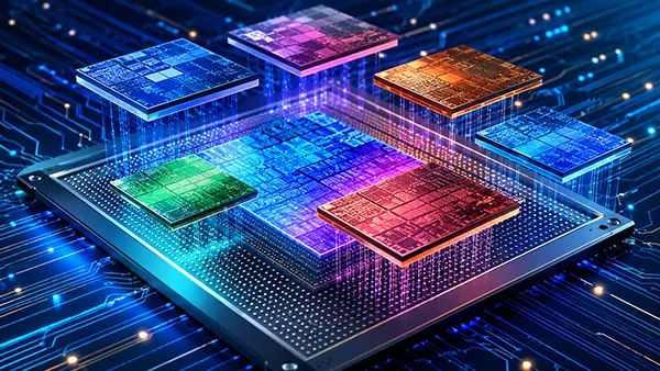
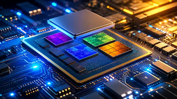
A chiplet-based processor divides major functions into separate silicon dies connected through high-speed interconnect technologies. Instead of creating a single large processor, manufacturers assemble several specialised chiplets within one package. These components communicate with each other at extremely high bandwidth and low latency, allowing the processor to function as a unified system.
One of the most important advantages is manufacturing efficiency. Smaller dies typically achieve higher yields because defects affect a smaller area of silicon. If one chiplet fails quality testing, only that component must be replaced rather than discarding an entire large processor. This significantly improves production economics.
Chiplets also allow different manufacturing nodes to coexist within the same package. A processor may use advanced 3 nm CPU chiplets alongside 6 nm or 7 nm input/output chiplets. This strategy balances performance and cost while allowing manufacturers to allocate expensive leading-edge silicon only where it provides measurable benefits.
Real-World Adoption Across the Semiconductor Industry
AMD played a major role in popularising chiplet architecture through its Ryzen and EPYC processor families. The company demonstrated that modular designs could compete successfully against traditional monolithic processors while improving manufacturing efficiency and scalability.
Intel has expanded its own modular strategy through technologies such as Foveros and EMIB, enabling the integration of multiple dies within advanced packaging systems. These approaches support heterogeneous computing environments where different chiplets perform specialised tasks.
By 2026, chiplets are no longer limited to CPUs. Artificial intelligence accelerators, graphics processors, networking hardware and data-centre solutions increasingly rely on modular packaging technologies. Industry initiatives such as the Universal Chiplet Interconnect Express (UCIe) standard are further encouraging interoperability between chiplets developed by different organisations.
The Future Impact of Modular Processor Design
The shift towards chiplets is reshaping the economics of semiconductor development. Companies can reuse proven chiplet designs across multiple product generations, reducing development time and lowering engineering costs. This reuse model resembles software development practices, where modular components accelerate innovation.
Data centres are expected to benefit substantially from the trend. Modular architectures allow hardware vendors to create processors tailored to specific workloads such as machine learning, cloud services, high-performance computing or edge infrastructure. This level of customisation would be significantly more expensive using traditional monolithic designs.
Consumer devices may also gain advantages. As packaging technologies mature, chiplets could enable more powerful laptops, workstations and mobile devices while maintaining manageable manufacturing costs. Greater flexibility in design may lead to faster product cycles and more specialised computing solutions.
Challenges That Still Need to Be Addressed
Despite its advantages, chiplet technology is not without challenges. High-speed communication between separate dies requires advanced packaging methods and sophisticated interconnect standards. These technologies introduce additional engineering complexity that manufacturers must carefully manage.
Software optimisation remains another consideration. Although chiplet-based systems generally appear as unified processors to operating systems, developers increasingly need tools that can fully exploit heterogeneous computing resources distributed across multiple specialised dies.
Nevertheless, industry momentum strongly favours modular architectures. As manufacturing costs continue to rise and demand for artificial intelligence, cloud computing and advanced data processing expands, chiplets provide a practical path for sustaining performance growth. By 2026, they have evolved from an experimental concept into one of the most important foundations of modern processor design.